Prototyping Toolbox Series: PCB Design

Treetown Tech
At Treetown Tech, in-house PCB design is an important tool in our product development arsenal. Want to learn more about how we do it? Read on!
At Treetown Tech, in-house PCB design is an important tool in our product development arsenal. Want to learn more about how we do it? Read on!

Printed circuit boards (PCBs) are ubiquitous these days. Reading this post on your phone? Wearing a smartwatch? Well then, you’ve got some PCBs right on your person! You’ll find PCBs in nearly every electronic product— from laptops to cars, gaming consoles to medical imaging equipment. PCBs are even finding their way into more and more household items like lightbulbs and fans as more gadgets connect to the internet via “smart” connected systems.
At Treetown Tech, in-house PCB design is an important tool in our product development arsenal. Want to learn more about how we do it? Read on!
A printed circuit board, or PCB, is a board that connects various electronic components within a device to implement an electronic circuit. Instead of a rat’s nest of wires connecting electrical components, a PCB creates the electrical connections with copper, or traces, all housed within a rigid board. (Flexible boards also exist, but that’s for another day.) Simple applications may have just a few components, but complex boards could house thousands upon thousands!
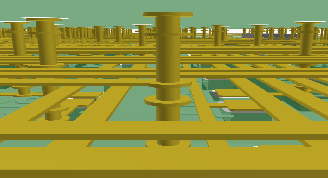
Boards can have components on one or both sides and are often constructed in multiple layers, especially as they grow in complexity. This means an increased density of components and smaller form factors. Multilayer boards have a copper layer sitting on a substrate layer, which is then stacked one on top of another, like an electronic lasagna.
At Treetown Tech, our electrical engineers are well-versed in PCB design. But where do we begin a new project?
Designers begin by asking and answering, “What do we want this device to accomplish?” Setting requirements allows us to start piecing together different types of components, such as sensors, microcontrollers, resistors, capacitors, and power supplies, to accomplish the desired function. Each component has a data sheet with specs for how it works, communicates, and needs to be powered.
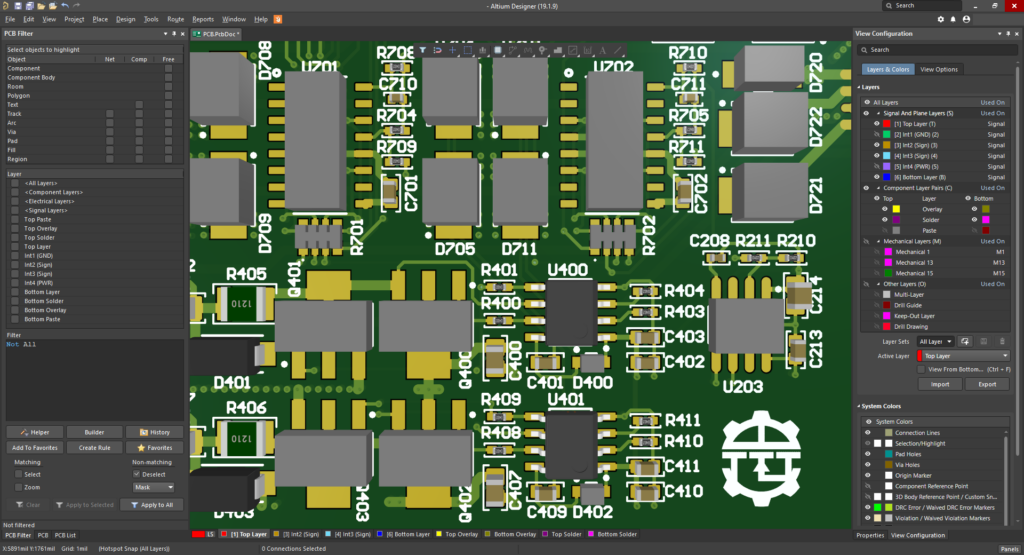
Our team then uses Altium Designer, a top electronics CAD design tool, to create a board schematic. Depending on the design’s simplicity, we can create PCBs in as little as a day. Very complex designs, however, can take a couple of months as we finalize components and how they interface. Our most intricate board, which was designed, tested, and modified over the course of many months, originally consisted of a whopping 16 layers, but with lots of thought, design, and testing, we reduced it to 10. Our team has decades of experience in PCB design and brings creative ideas to the table, which is especially important today with many PCB components being in short supply.
The next phase is the layout, where we set the size of the PCB (usually driven by other system requirements, such as the physical space allocated), place the components on the board, and then connect all the components with traces. It’s like laying out a very complicated city and connecting everything with tiny copper infrastructure—like roads, bridges, and utilities!
The design process is a cycle of methodical building and fast prototyping part by part to make sure each one works before we put together the full board.
At Treetown Tech, we work across several industries, including automated truck delivery, EV charging, manufacturing lines, and medical wearables. As you shrink in size from a delivery truck to a golf ball, the board needs to shrink too. And that’s not easy.
Deciding when to create custom electronics is a complex, nuanced process. We look holistically at a project—not just its electrical needs—to solve high-risk problems first. This can involve prototyping with off-the-shelf electronics (think Raspberry Pis) or smaller test PCBs that are research rather than development-oriented. Basically, we need to learn as quickly as we can without sinking resources into a complex layout before we’ve actually arrived at a solution.
Like everything technical at Treetwon Tech, this process stays in contact with the full business need, from customer discovery to how we’re going to manufacture at scale.
While sometimes we just do custom PCB design, more often, our projects have software, electrical, and mechanical design needs. This is especially useful when we create custom PCBs since we can write all of the firmware and software to interface with our new PCBs, as well as design the custom housings and even create thermal simulations of our boards—all in-house. With everything under one roof, we stay nimble in implementing each product feature—software or hardware—and keeping costs down and production speedy. It’s all part of our iterative, team-based design approach. Let us know if we can help with your next electronics project!
You have the vision. We have the team and expertise to get it built. Let's collaborate to innovate, problem-solve, and de-risk every step of the way.